Laser・Semiconductore manufacturing equipment・Metal additive manufacturing|Room temperature wafer bonding machines|Room temperature wafer bonding machines
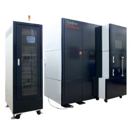
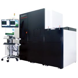
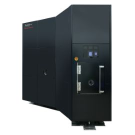
Room Temperature Wafer Bonding Machine BOND MEISTER
The handling companies : Nidec Machine Tool Corporation
- Contact information for product inquiry
- Contact Us
Room temperature wafer bonding machine opens up new horizons in the bonding process.
Two wafers can be securely bonded at room temperature... This room temperature bonding method based on surface activation is like a dream come true.
Room temperature bonding technology originated in Japan and has been studied for many years.
Today, the application fields for room temperature bonding are rapidly expanding due to the simple process and wide range of applicable materials.
Room temperature bonding is of great use in research and prototyping as well as actual device production.
BOND MEISTER is a bonding device worthy of the name MEISTER (master craftsman), and is the result of combining the manufacturing technology and bonding process technology that we have developed over many years.
We will continue to support our customers' device development efforts by providing equipment with high reliability and bonding quality, and bonding support services that are integrated with our technical capabilities.
- Principle and features
- Application of room temperature bonding
- Bonding case study
- MWB-04/06-R
- MWB-04/06/08-AX
- MWB-08/12-ST
- Device product lineup
- Support for customers
bond mate
Principle and Features
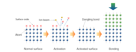
Principle
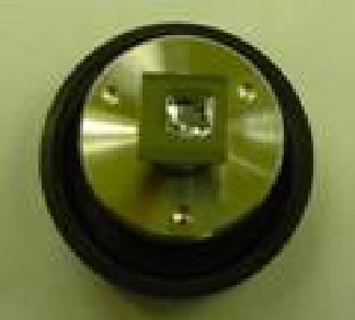
The surface of the bonding material is irradiated with an ion beam or neutral atom beam in a high vacuum.
This removes the oxide film and adsorbed layer on the material surface, revealing the material's natural "bonding possibilities." This is called an "activated surface."
When the activated surfaces are brought into contact with each other, the bonding force works instantly and the two materials are securely bonded.
Features
A room temperature process that achieves bond strength equivalent to that of the base material.
Since thermal strain and thermal stress from bonding do not occur, it is easy to handle micro-sized workpieces and the quality of the device is stable.
No heating/cooling time is required, meaning that high throughput can be achieved.
A wide variety of materials can be bonded. Also, different materials can be bonded.
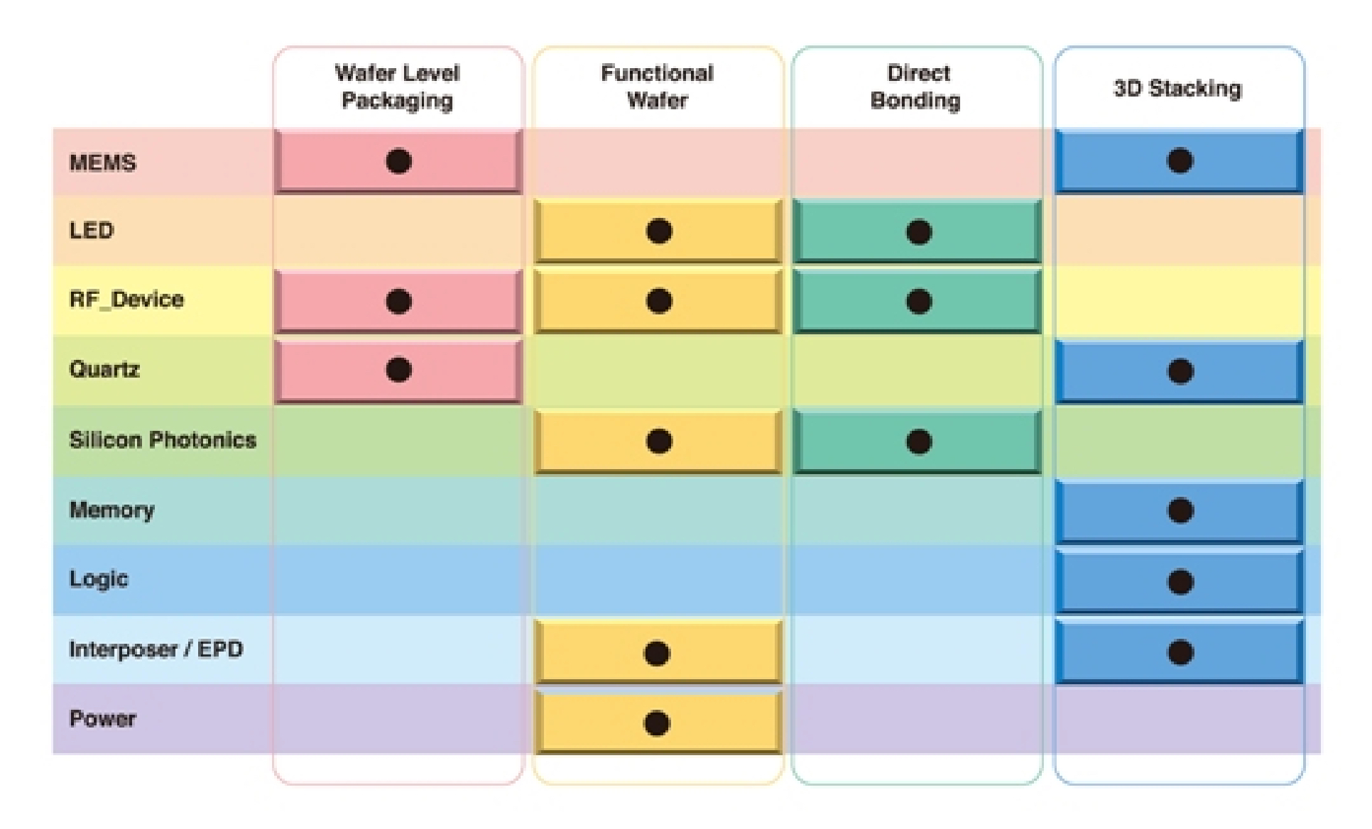
Application of room temperature bonding
Room temperature bonding is widely used in the following categories.
- Wafer level packaging
- Especially for MEMS and crystal devices, packaging can be achieved without heat distortion, resulting in improved device quality and lower cost.
- Manufacturing of functional wafers
- By bonding bare wafers of different materials, various types of functional wafers can be manufactured.
- Applications that utilize direct bonding
- Since intermediate materials such as resins or alloys are not required, direct bonding improves the device characteristics.
In addition, the cost for intermediate materials can be eliminated. - Wafer stacking
- Multiple layers of wafers with through-silicon vias (TSVs) can be bonded, enabling the manufacture of 3D integrated devices.
Since no heat is applied, device reliability is maintained at a high level.
Also, because there is no thermal distortion, the device's internal stress is minimized.
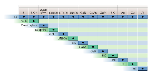
Bonding case study
Silicon-based materials
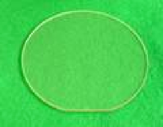
Silicon/Silicon
Uniform bonding of full-face voidless achieves the same strength as the base material.
Since glass materials with different coefficients of thermal expansion are not used, encapsulating packaging is possible using only silicon.

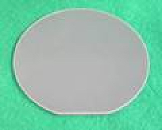
Silicon oxide film/Silicon oxide film
Used for packaging that requires insulation.
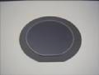
Wafer-level packaging for acceleration sensors
This is an example of wafer-level packaging using three-layer bonding, where the device wafer is sandwiched between sealing wafers above and below.
Oxide-based materials
Quartz glass/Quartz glass
This technology can be applied to the development of optical elements.
Quartz glass/Silicon
Dissimilar materials can also be bonded. It is possible to integrate electronic devices and optical components.

Sapphire/Silicon
LiNbO3/Silicon
Even materials with very different thermal expansion coefficients can be easily bonded at room temperature.
The technology can be used for a wide range of devices such as high frequency devices and optical elements.
Compound semiconductors
GaN/Silicon
These materials show great potential for use in light-emitting devices and power devices.
With direct bonding, efficiency can be improved and costs can be reduced.

GaAs/GaAs
High-quality bonding is possible even for compound semiconductors.
In addition, these materials can be bonded to dissimilar materials to create silicon photonic devices.

SiC/Silicon
These materials show great potential for the next generation of power devices.
Direct bonding provides greater freedom in design and improved performance.
Metal materials
Au/Au
Two pieces of gold deposited on silicon are bonded together.
In tension tests, the base material has broken before the bond, indicating a strong bond.
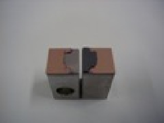
Cu/Cu
Two pieces of copper deposited on silicon are bonded together.
In tension tests, the base material has broken before the bond, indicating a strong bond.
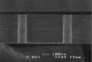
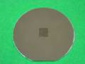
Through wiring bonding sample
Aluminum through wiring deposited on silicon wafers are bonded together.
Low stress bonding and high precision alignment can be achieved by applying room temperature bonding to wafer stacking.
Device specifications BOND MEISTER MWB-04/06-R
This is the standard model for a wide range of applications from research to device prototyping and small to medium volume production.
Processing is performed in units of 1 set (1 bond).
Achieves high throughput and semi-automation. This model can be used for medium-volume production of devices.
We offer all-in-one support for all transport and alignment functions, and easy-to-use PC-based operation that allows you to start using the machine from day one.
Special jigs can be used to bond wafers and chips of different shapes. This model can be used to bond a wide range of materials and devices.
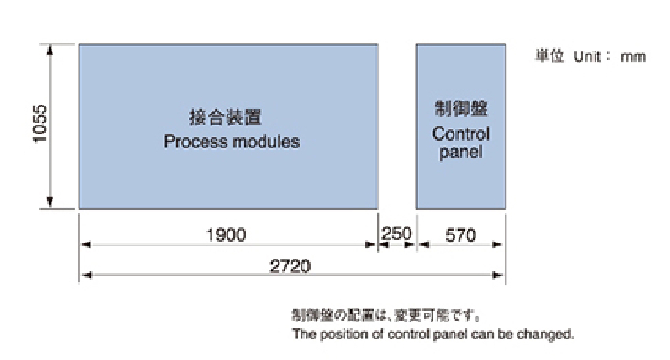
| Item | Specifications |
|---|---|
| Set wafer | 1 set |
| Wafer size | 100 mm/150 mm |
| Operation | Semi-automatic |
| Alignment accuracy | ±2 μm (MHI Machine Tools measured value (Note 1)) |
| Surface activation | Ion gun |
| Pressure welding mechanism | Max. 20 kN |
| Alignment | By IR transparent image |
| Degree of chamber vacuum | <1.0 × 10⁻⁵ Pa |
| Utility | Argon gas, nitrogen gas, compressed air Power supply (200 V, 100 V) |
(Note 1) Measured data values are not guaranteed values.
Device specifications BOND MEISTER
MWB-04/06/08-AX
This model is designed for mass production of devices and offers both high throughput and flexibility.
10 sets (10 bonds) are continuously bonded in cassette-to-cassette processing.
The powerful recipe management functions allow different parts and process conditions to be configured for each set. High-mix low-volume production can also be performed automatically.
Simply load the wafers in the cassettes and press the start button. The processing is performed automatically. Transport and alignment are all automatic.
Special jigs can be used to bond wafers and chips of different shapes.
This model can be used to bond a wide range of materials and devices. Flexible semi-automatic operation is also possible.
Option
AB gun activation unit
This unit enables further efficient metal materials bonding.
Heating/pressurizing chambers after bonding, heating and pressurizing are used to achieve even more reliable bonds.
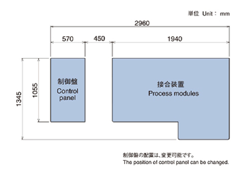
| Item | Specifications |
|---|---|
| Set wafer | 10 sets |
| Wafer size | 100 mm/150 mm/200 mm |
| Operation | Fully-automatic/Semi-automatic |
| Alignment accuracy | ±2 μm (MHI Machine Tools measured value (Note 1)) |
| Surface activation | Ion gun/FAB gun |
| Pressure welding mechanism | Max. 100 kN |
| Alignment | By IR transparent image |
| Degree of chamber vacuum | <1.0 × 10⁻⁵ Pa |
| Utility | Argon gas, nitrogen gas, compressed air Power supply (200 V, 100 V) |
(Note 1) Measured data values are not guaranteed values.
Device specifications BOND MEISTER MWB-08/12-ST
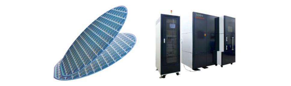
Room temperature wafer bonding machine for 300 mm wafers
This powerful room temperature wafer bonding machine offers 3D stacking of various types of IC and memory, and mass production of CMOS image sensors.
This model is a bonding device for full-scale 3D stacked devices.
Since bonding is performed at room temperature, differences in thermal expansion coefficient between wafers are no longer a problem, and high alignment accuracy is assured.
A wide range of materials can be joined, including copper, gold, aluminum, and other metals, silicon materials, compound semiconductors, and monocrystal oxides.
Since heating/cooling is not required, the machine is capable of high throughput production.
It is highly automated.
All operations, such as transport and alignment, are performed automatically by simply loading the wafers into the dedicated cassettes.
The recipe can be adapted for each wafer to be bonded, so even if wafers of different parts are mixed together, the bonding process can be fully automated. This model can also handle high-mix low-volume production.
Supports 200 mm wafers.
This model features a high-load pressure welding mechanism.
It is capable of applying a pressure of up to 200 kN (20 tonnes), which is used especially for metal bonding where high loads are required.
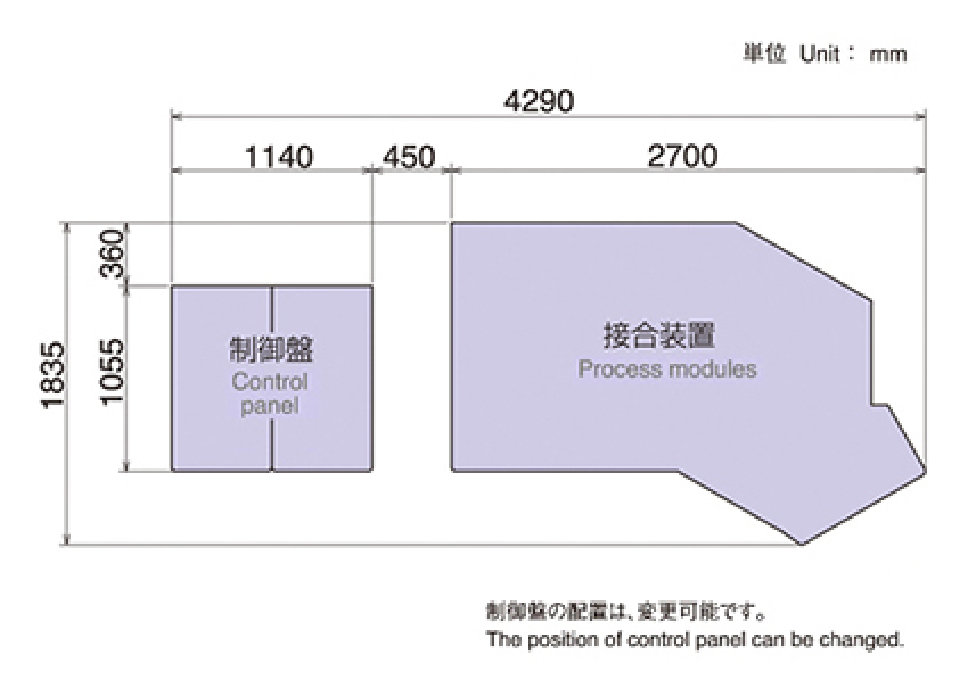
| Item | Specifications |
|---|---|
| Set wafer | 5 sets (max.) |
| Wafer size | 300 mm/200 mm |
| Operation | Fully-automatic/Semi-automatic |
| Alignment accuracy | ±2 μm (MHI Machine Tools measured value (Note 1)) |
| Surface activation | Argon fast atom beam |
| Pressure welding mechanism | Max. applied load 200 kN |
| Alignment | By IR transparent image |
| Degree of chamber vacuum | <1.0 × 10⁻⁵ Pa |
| Utility | Argon gas, nitrogen gas, compressed air Power supply (200 V, 100 V) |
(Note 1) Measured data values are not guaranteed values.
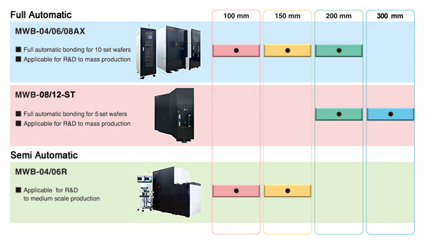
Device product lineup
We offer a range of products to suit your operations.
Wafer sizes from 100 mm to 300 mm are supported.
All machines are equipped with an integrated transport and alignment system and are ready to begin production immediately after installation.
They feature an easy-to-understand operating system and can be operated by anyone quickly and easily.
The powerful production management features such as recipe management and log management ensure reliable quality control.
Advantages of choosing BONDMEISTER
Bonding without thermal distortion results in significantly higher yields.
The ability to bond a wide variety of materials gives a great deal of flexibility in device design.
Since there is no thermal distortion, devices can be made smaller and thinner, increasing the yield per wafer.
Strong bonding minimizes the bonding area and increases the yield per wafer.
Direct bonding eliminates the need to use resin or metal as an intermediate material, thus reducing costs.
No special utilities are required, keeping running costs low.
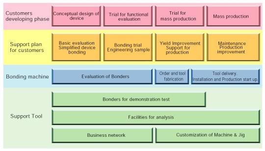
Support for customers BOND MATE
Development support system for customers
We offer a comprehensive support program, BOND MATE, to assist customers who are developing devices using room temperature bonding. We can provide a full range of support, from the initial examination of materials to the start of mass production and after-sales service.
By utilizing our analysis and evaluation facilities and process engineers, we are able to provide bonding support tailored to your development phase.