Nidec Advance Technology Corporation
Business Summary
The features of our main product line.
Credibility built on market-proven technology.
Technology developed in order to meet market needs has been contributing in the production lines around the world.
Born out of the need for high-speed, high-accuracy measurement/ inspection of fast-evolving electronic components, NIDEC ADVANCE TECHNOLOGY products reflect the culmination of our longstanding experiences in a variety of elemental technologies. Our technical portfolio today realizes extensive application in:
- mission-critical, high-performance integrated circuits and associated software
- hardware design enabling submicron control
- component fixture operation for processing and assembling multi-pin and narrow-pitch chips, and
- two- and three-dimensional optical imaging and three-dimensional process technology
NIDEC ADVANCE TECHNOLOGY’s main strength derives from the ability to blend a wide range of elemental technologies to the industry's highest level of performance.
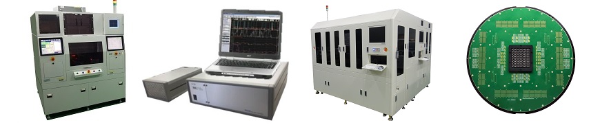
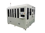
Automatic Test Equipment
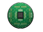
NIDEC ADVANCE TECHNOLOGY GATS (Grid Array Testing System) series carry out open/leak circuit tests on semiconductor package (MCM/CSP/BGA). NIDEC ADVANCE TECHNOLOGY offers an array of testing equipment used to conduct open/leak tests on motherboards, as well as many other printed circuit boards. NIDEC ADVANCE TECHNOLOGY provides open/leak inspection system for touch screen panel and LCD, at singulated size to multifaced size, making use of our diversed contact & non-contact technologies.
Electrical Tester
NIDEC ADVANCE TECHNOLOGY testers undertake various types of continuity tests at broad voltage and resistance levels.
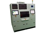
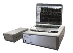
Fixture and Software for Open/Leak Inspection
In addition to jigs and fixtures for probing conductors and electrode pads, NIDEC ADVANCE TECHNOLOGY provides specialized software for test point selection and log analysis.
Automated Optical Inspection Equipment
NIDEC ADVANCE TECHNOLOGY's inspection systems serve to locate open/leak circuits on printed substrates forming different conductor patterns within photomasks and inner/outer layers. These vision inspection systems are also used to measure the shape of via holes and solder bumps and to find scratches and stains on them.
Probe Card
Our probe cards are a perfect solution for advanced wafer testing challenges.